Lab 1 - EE 420L
Authored
by Tyler Ferreira,
ferret1@unlv.nevada.edu
January 24, 2017
Pre-lab work
- Your lab reports will be drafted using html and placed on CMOSedu.
- Prior to the first day of lab, but no earlier than one week before the lab starts, request a CMOSedu account, using your UNLV email address, from Dr. Baker (rjacobbaker@gmail.com).
- Review the material seen here covering editing webpages (do this before the first lab).
- Read the entire write-up seen below before coming to lab
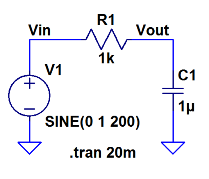
Experiment 1
Figure 1.21
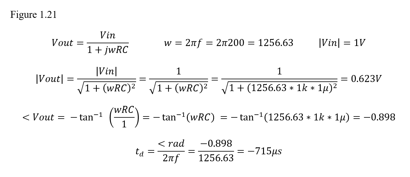
Hand Calculations
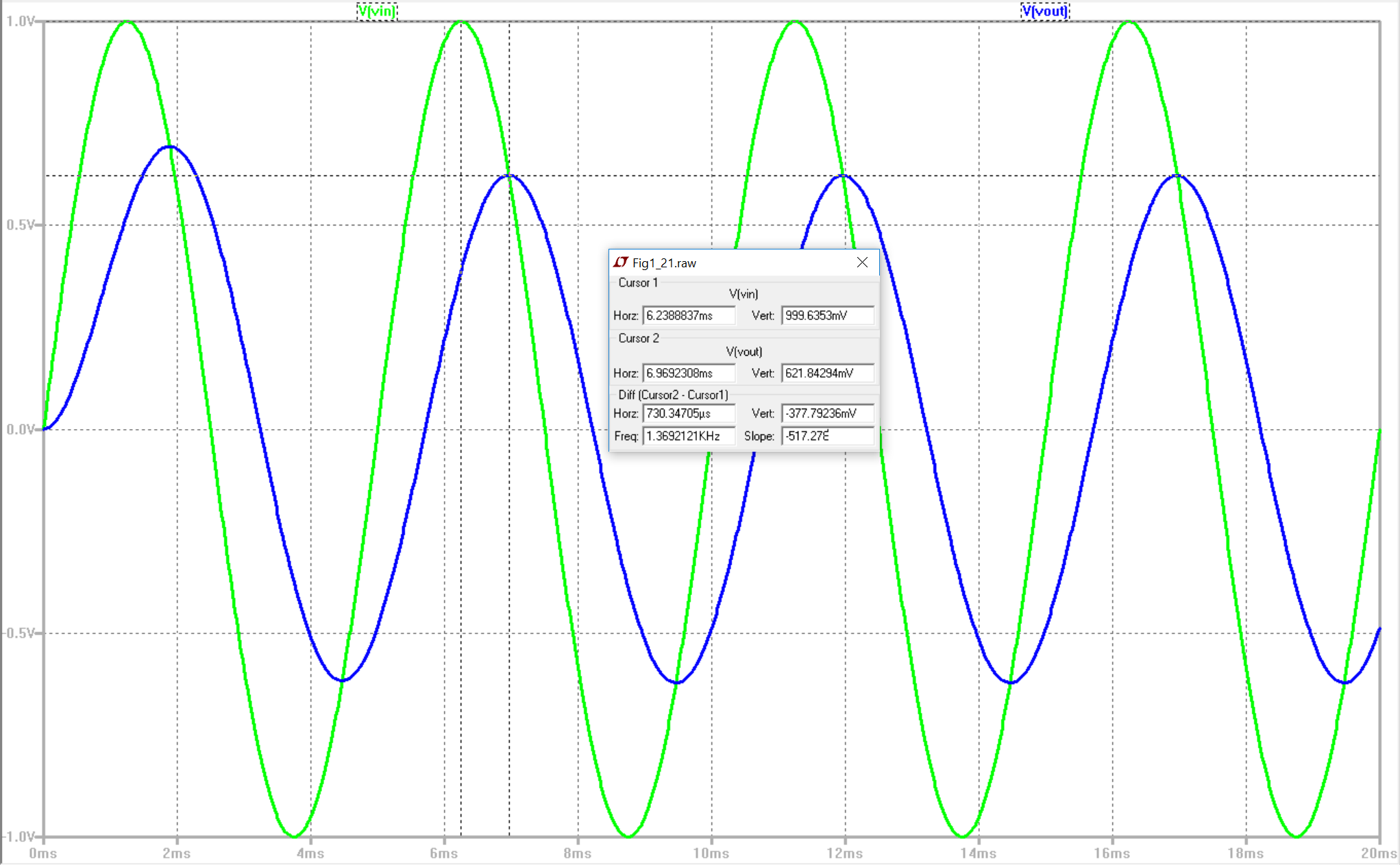
Spice Simulations of Figure 1.21
Scope Waveforms
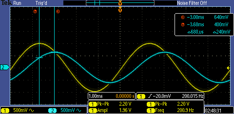
Comparing my handwork, simulation results, and my experimental results:
| Handwork | Simulations | Experimental |
| Magnitude of Vout | 623 mV | 622 mV | 640 mV |
| Time Delay | -715 µs | -730 µs | -680 µs |
All of my results are similar to each other with less than 10% deviation from each other.
The negative time delay means that the output signal will lag behind the input signal.
Experiment 2
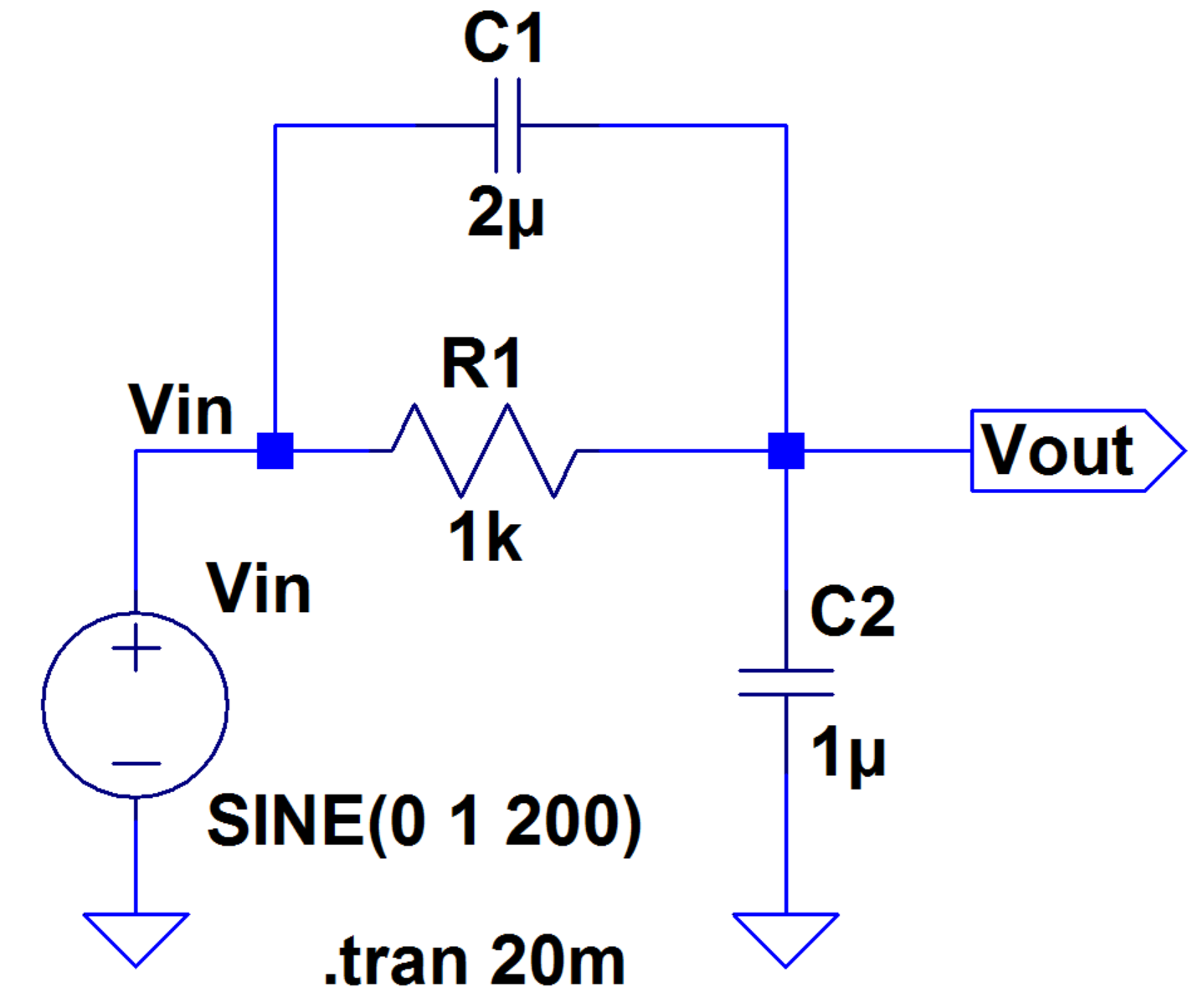
Figure 1.22
Hand Calculations
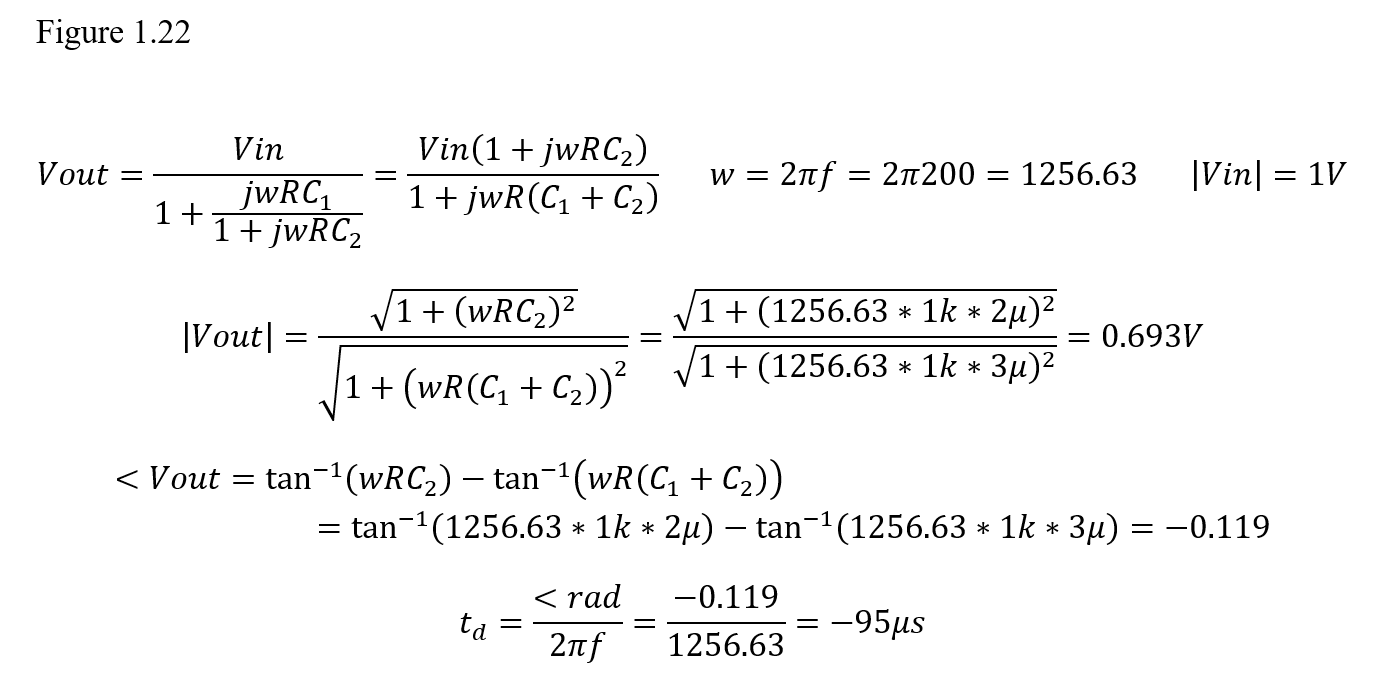
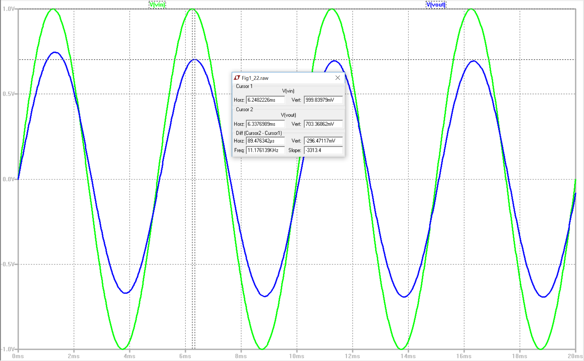
Spice Simulations of Figure 1.22
Scope Waveforms

Comparing my handwork, simulation results, and my experimental results:
| Handwork | Simulations | Experimental |
| Magnitude of Vout | 693 mV | 703 mV | 740 mV |
| Time Delay | -95 µs | -89 µs | -100 µs |
All of my results are similar to each other with less than 10% deviation from each other.
The negative time delay means that the output signal will lag behind the input signal.
Experiment 3
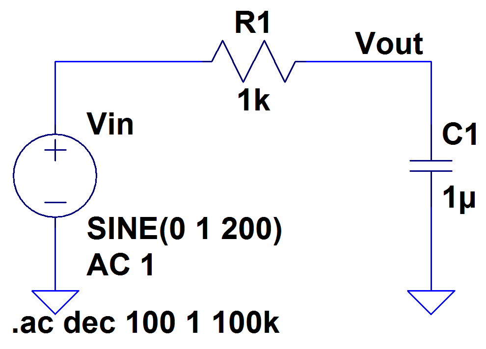
Figure 1.24
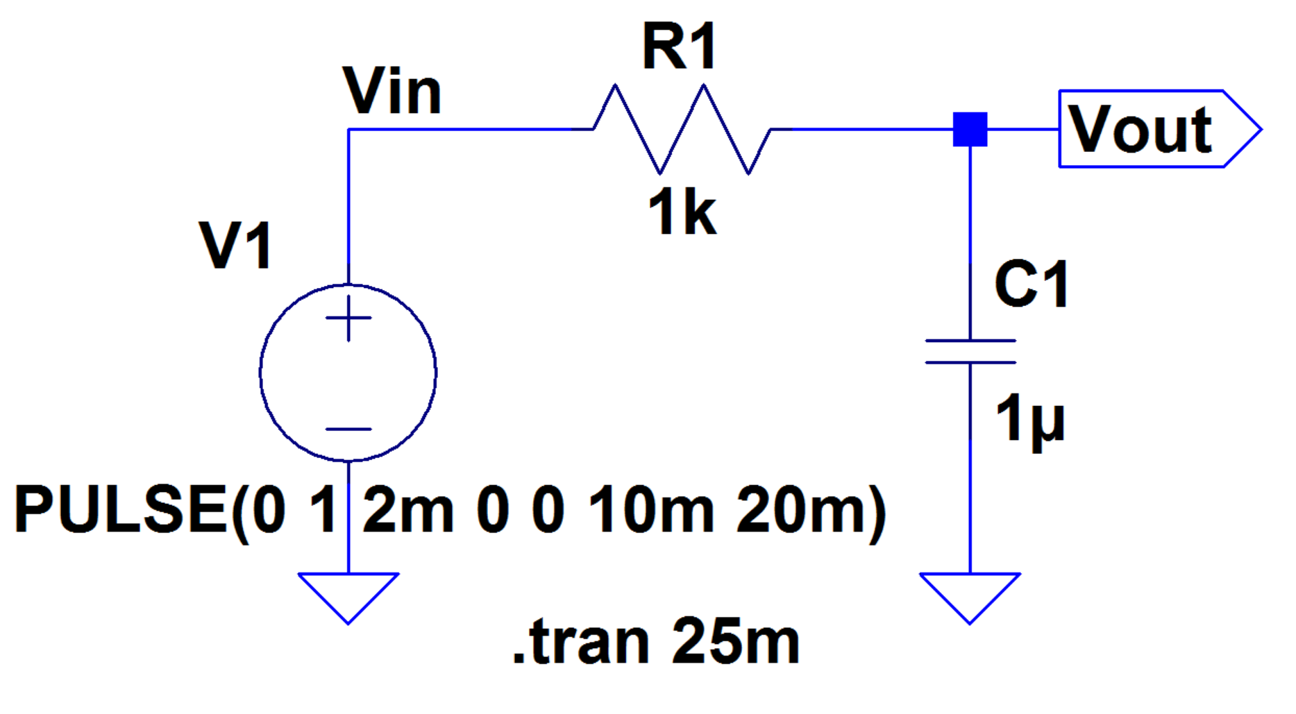
Hand Calculations
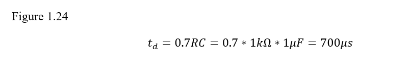
We can use this equation to find the time delay because the input signal is a step function.
Spice Simulations of Figure 1.24
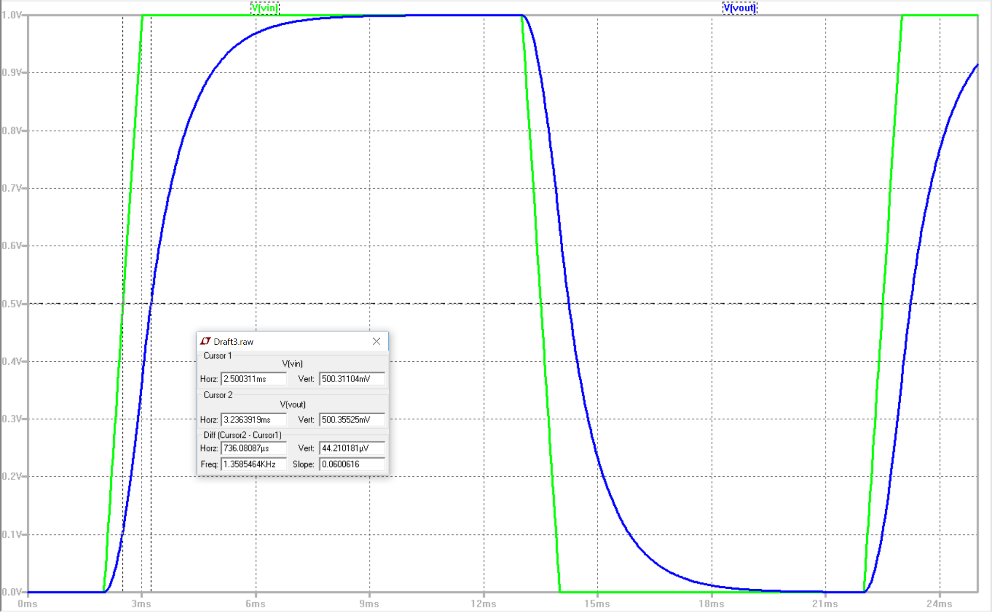
Scope Waveforms
For a time delay involving a step voltage we take the time at 50% of the input voltage.
Comparing my handwork, simulation results, and my experimental results:
| Handwork | Simulations | Experimental |
| Time Delay | 700 µs | 736 µs | 660 µs |
All of my results are similar to each other with less than 10% deviation from each other.
Experiment 4
Figure 1.23
Spice Simulations of Figure 1.23
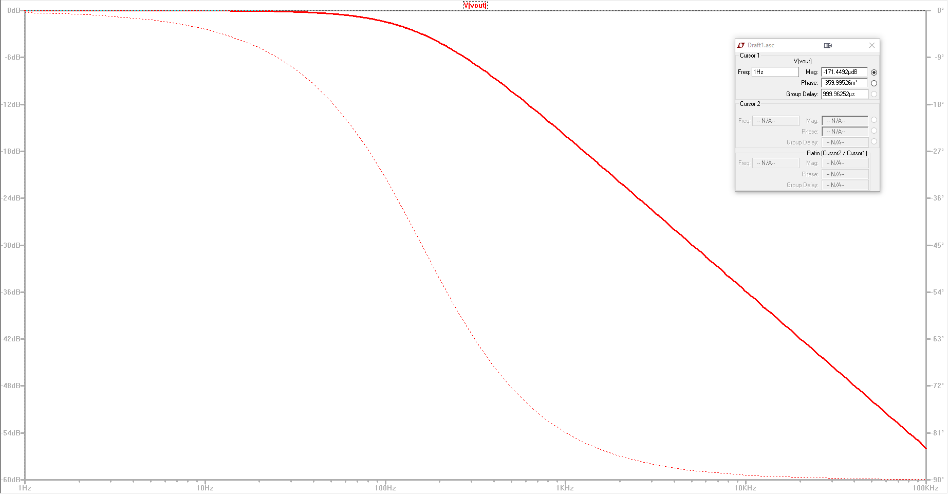
I will take this plot and move the cursor to different values and list them in the table below.
| Frequency | Magnitude | Phase |
| 1 Hz | -171.45 µdB | -360m° |
| 159.78 Hz | -3.02 dB | -45.08° |
| 1 kHz | -16.09 dB | -80.98° |
| 10 kHz | -36.00 dB | -89.09° |
| 100 kHz | -55.96 dB | -89.90° |
I will backup all of my work on my OneDrive and my Desktop.

Return to the directory listing of my labs
Return to the directory listing of students in EE 420L, Spring 2017
Return to the EE 420L, Spring 2017 webpage